
Custom thumbnail...
Introduction
Hello it's a me Drifter Programming! Today we continue with my small series, where we will be implementing a complete system in VHDL. Today's post is the third part of the series and so I highly suggest you to go read the previous parts first, where I explain and analyze the system and also implement the first "part" of the system (the so called "step 1"). The second step contains ROM and so I highly suggest you to read my post about that!
Today's post will be about:
- implementing the calculation step of the result vector R (step 2)
So, without further do, let's get started!
Small Recap
In my previous post we talked about the implementation steps that we will use and also did the first step. In this first step we implemented the storage of vector A and so the 2 first states of the FSM.
In total we have to implement the following mathematical operation:

or

where:
- A is a line vector of M elements
- H is a MxN matrix
- the result matrix R has N elements
- the multiplication is in modulo 2 (AND for multiplication, XOR for addition)
- the elements of the matrices are 1-bit in length and so only 0 or 1
The result-element gets calculated as:

To make the AND operation and XOR happen in one single step we will need an Accumulator that stores the previous result in a register and applies the XOR operation between the "current" and "previous" multiplication (AND) result. Using a reset signal we have to make sure that the previous result 0 (zero) for the first calculation! That way the whole calculation process will only take MxN-steps, which is the number of elements in vector H.
This is the second part of the implementation and is what we will be implementing today! For this step we extend our system by inserting two more memories, which are ROM(H) and RAM(R) together with their counters (counterH, counterR). We also have to implement the accumulator which does the main operation of the system. Lastly, we also extend the FSM of our system.
Step 2
Let's get started with the second step, which is the most important one!
Last time we considered that M = 4 which meant that vector A contains 4 elements. The actual address-length and count-length of the corresponding counter was logM = 2-bits. Let's say that we want to store 8 elements in ROM (H), which means that MxN = 8-elements and so N = 2-columns.
And so we need:
- logMxN = log8 = 3-bits for the address and counter of ROM (H)
- logN = log2 = 1-bit for the address and counter of RAM (R)
This means that we will calculate something in the form:

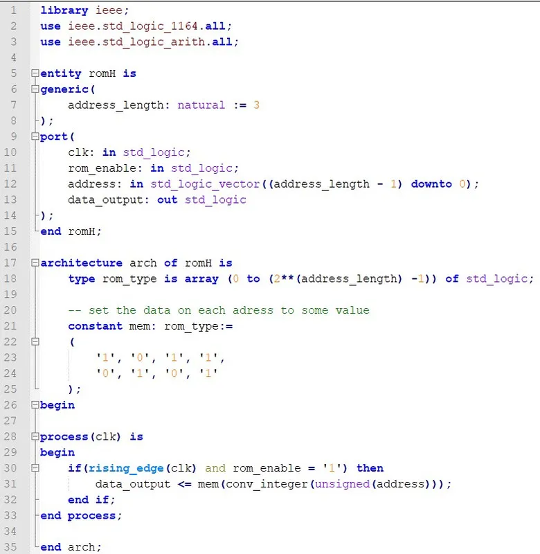
As already told last time, vector H will be stored in a ROM and will be static.Let's consider the following "random" matrix to be H:

This matrix will be stored column-by-column, so that the calculation can be done easily by just using one single counter. By storing the previous matrix like that we end up with the following code for ROM(H):
RAM(R) which will store the result vector R[N] is exactly the same as RAM(A) and we only have to change the generic address parameter which now will be 1-bit so that we are able to store N = 2-elements. The RAM code looks like this:
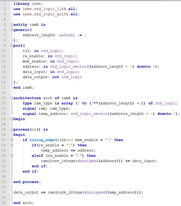
Note that something is different then last time, will explain why in a bit!
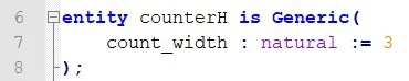
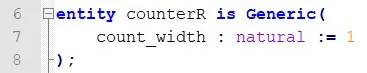
The corresponding counters of the two new memories are exactly the same as the counter for RAM(A) and we just have to change the generic parameter like that (for each one):
The final and last "new" component is the accumulator which will do the actual calculation. The accumulator has to do a AND operation between the values of the memories (A[i] and H[j][i]) which will be inputs of the component. After it does a XOR operation of the result of this "new" AND operation together with the previous one, which at first has to be initialized by a reset signal to '0'. Storing the "previous/temporary" result in a register can be done very easily by defining a signal that only changes via the clock (synchronous). That way the accumulator component in VHDL is:
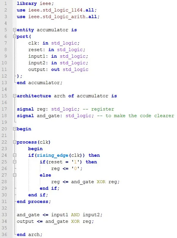
You can see that there is a synchronous reset with which the register will be initialzed to '0' every time we start a new multiplication of line-column or every time RAM(R) gets written (N-times in total). The value of the register is equal to the XOR result between the AND of the inputs and the previously stored value of the register. The reset signal has to be controlled by the FSM.
Control Unit
Let's now get into the new FSM!
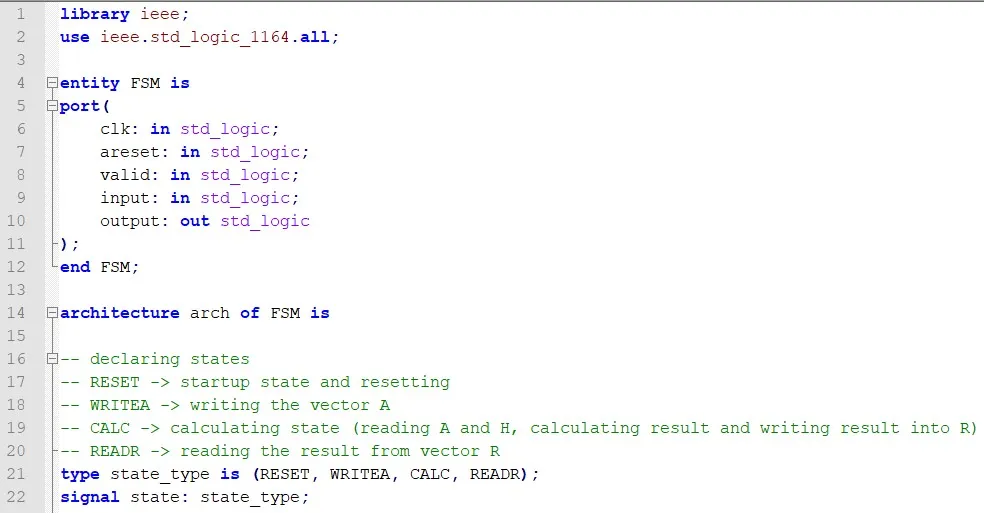
First of all, the inputs/outputs are the same and are still the main inputs/outputs of the whole system (this will change next time, where the FSM will be made into a component). You can see that we now have all 4 states. The two new states are:
- CALC, where we will be reading from RAM(A) and ROM(H) , calculating the multiplication result and storing the result in RAM(R)
- READR, where we will be reading the result from RAM(R). This last state was actually meant to be done next time, but why not get rid of it now? Haha.
Our FSM now has the following control signals:
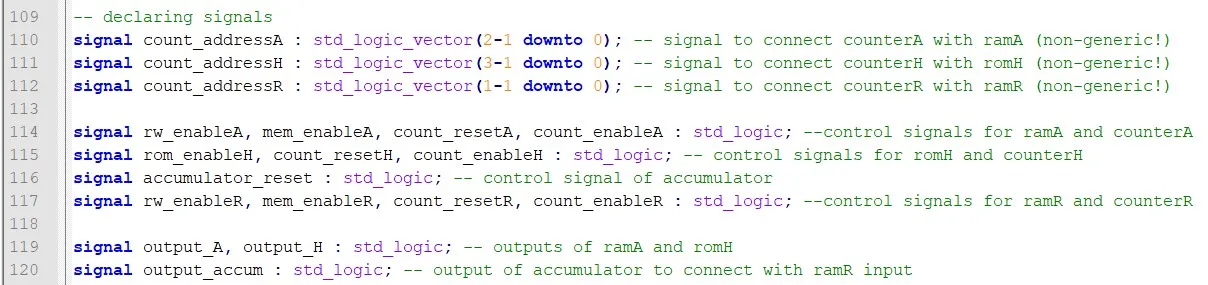
You can see that the new RAM(R) has the same signals as RAM(A) that we covered last time. All counters also have the same signals as counterA that we covered last time. ROM(H) only has one signal, which activates the memory for reading. We also have a control signal for the accumulator, which resets the register/signal to '0'. Lastly we also need 3 "wire-signals" which are useful for connecting the outputs of RAM(A) and ROM(H) with the inputs of the accumulator, and also for connecting the output of the accumulator with the input of RAM(R).
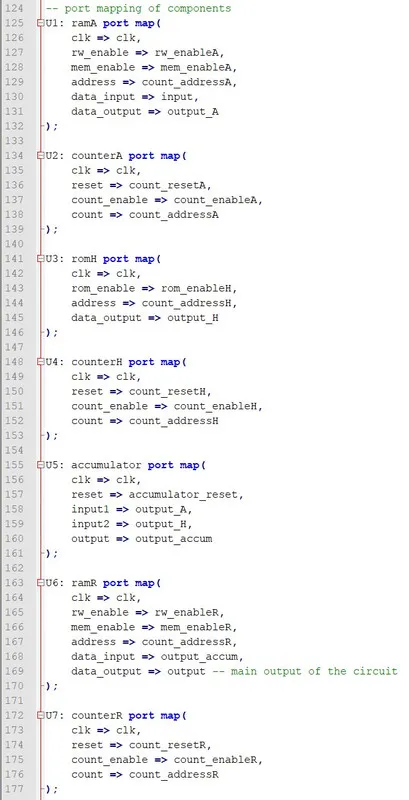
You might have seen that I skipped out of the components :P, but either way here the "new" port mappings:
The FSM still has 2 processes: one that controls the state transitions and one that controls the outputs/control signals. The new state transitioning process is:
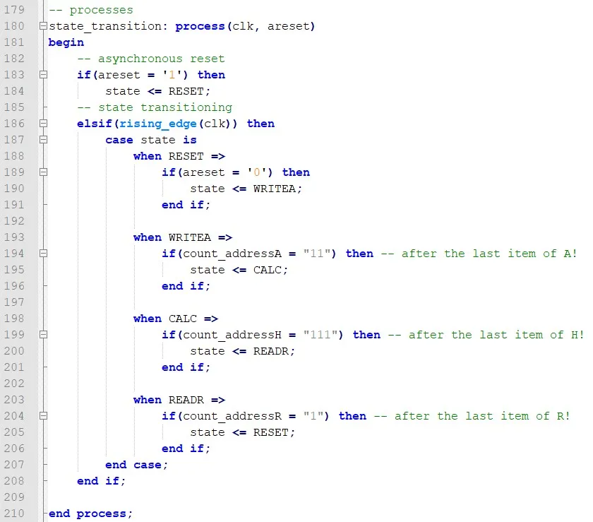
The actual condition of transitioning in the CALC state is being in the last item of ROM(H), which is of course easy to understand, cause the multiplication will be done after reaching this element. Note that the actual storage and calculation always happens in the "next cycle", which means that transitioning in the last item, doesn't mean that we don't "include" it in the calculation process. The condition of READR is being in the last item of vector R, similar to the condition we had for WRITEA.
The most important process though, is the one about the control signals. The first two states of our system, don't change a lot in behavior, but the individual "newly" added components will also need be to controlled by the RESET and WRITEA state now.

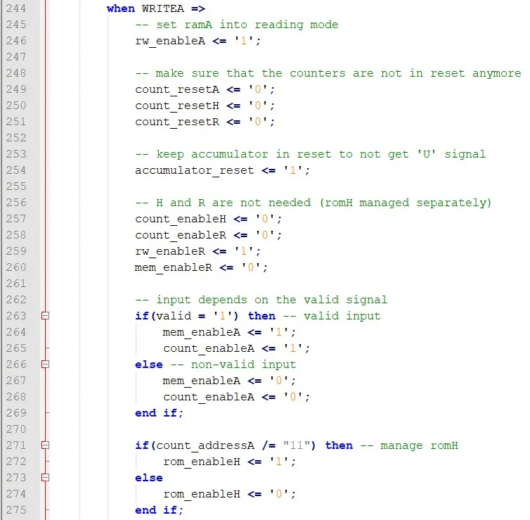
You can see that the "cases" of the 1st implementation step now change, because of the new control signals. Worth noting is that I "activate" ROM(H) when being in the last item of A in the WRITEA state. I did this, because the calculation in the accumulator takes place somewhat "asynchronous". By that I mean that we end up with a 'U' signal (undefined), which means that the register initialization "fails". To fix this I read the value of the ROM(H) in the previous cycle, cause the counter is already "ready" for reading the first item.
Let's now get into the CALC state:
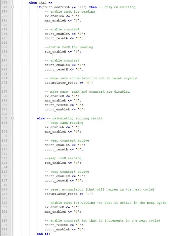
This state is very interesting. There are two cases:
- We are calculating only
- We are calculating and storing the result
For both cases we keep the two memories active for reading, but the storing memory RAM(R) is only activated when being in the last item ("11" in counterA for us). When storing the result we also reset the accumulator. The actual storage and reset/initialization happen in the next rising edge and so in the "next cycle" in some way, which means that we again don't lose any element of the matrix and actually store the final result of the calculation. Exactly when storing and re-initializing we "change" column in vector H.
The last state is:
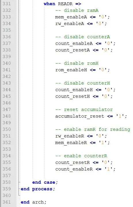
Very simple. We just have to "disable" everything except RAM(R) and the corresponding counterR. By enabling RAM(R) for reading I found during the simulation process that I did something wrong (also told before). The actual "reading" procedure happens in the next cycle and so the RAM's needed more then one cycle for reading! To fix this let's put the actually assigment of the output outside of the process. This doesn't make the RAM asynchronous! The actual "position" (temp_address) is still in the process like that:

Simulation
By inputing the same vector A as last time ("1111") what will the result be?

By using the software-model (C-code) we get:
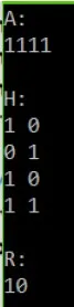
which means that the correct output is R = "10".
By simulating the circuit with ModelSim we get:

The whole simulation is large, but you might see that the system outputs '1' and then '0' in the READR state and that RAM(R) contains "10" which is the correct result! Note that we "read" in the next cycle and so the "last" element of the result vector is in the output, when reaching the RESET state again.
In this article I don't put the code as "text", but made screenshots. You can download the code from the following links on pastebin:
- ramA -> https://pastebin.com/dMhVfiHs
- ramR -> https://pastebin.com/yBLe5CEX
- romH -> https://pastebin.com/iurTf89u
- counterA -> https://pastebin.com/N5WAsVqi
- counterR -> https://pastebin.com/4b9w6EB4
- counterH -> https://pastebin.com/S7Smsy3N
- accumulator -> https://pastebin.com/jiGVZ7TD
- FSM -> https://pastebin.com/pZk0EmVA
Next time I will upload a .zip file with all the code from the series (all steps)...
References:
- For the mathematical equations I used quicklatex!
- The code is all written by myself (it's a task for my University)
Previous posts of this series
- Part 1 -> problem, analysis, software model, architecture
- Part 2 -> explaining how our architecture works, splitting the implementation in steps, implementing the storage step of vector A (step 1)
And this is actually it for today's post! I will see you next time again where we will get into the final (4th) step of the implementation process.
Bye!