
Custom thumbnail...
Introduction
Hello it's a me Drifter Programming! After the examinations of the week, me and all my friends where totally exhausted (or tired) and so we went to another city yesterday by car and where out for coffee, drinks and food all day since Friday. That's why I didn't had time for posting, cause I simply weren't home :P Eitehr way, today we continue with my small series, where we will be implementing a complete system in VHDL. Today's post is the second part of the series and so I highly suggest you to go read the previous part first, where I explain and analyze the system. I also set up a architecture for the system in Hardware, which means that the post is very important! The first step of the implementation contains a RAM component and so you should also read the post about that!
Today's post will be about:
- explaining how our architecture works
- splitting the implementation in steps
- implementing the storage step of vector A (step 1)
So, without further do, let's get started!
Small Recap
Let's first get back into what we actually have to solve!
We have to implement the following mathematical operation:

or

where:
- A is a line vector of M elements
- H is a MxN matrix
- the result matrix R has N elements
- the multiplication is in modulo 2 (AND for multiplication, XOR for addition)
- the elements of the matrices are 1-bit in length and so only 0 or 1
By analyzing the system we found out that each result-element gets calculated as:

To make the AND operation and XOR happen in one single step we will need an Accumulator that stores the previous result in a register and applies the XOR operation between the "current" and "previous" multiplication (AND) result. Using a reset signal we have to make sure that the previous result 0 (zero) for the first calculation! That way the whole calculation process will only take MxN-steps, which is the number of elements in vector H.
This is also the main and most important part of our architecture. For the rest please just read the corresponding post :P
How our architecture works
At first (RESET state), we reset all the components, which means that all registers, counters etc. will have to get a value of "zero". After that we disable the reset signal and go to the WRITEA state, where we enable RAM(A) for writing and start writing the input bits into it, but only if the valid signal is '1', which means that we have a correct input. Also, the counter of A has to be enabled (active for incrementation) only when the input is valid and else has to stay in the "current" value. Because the system is synchronous the reseting, writing, reading, switching states etc. will happen at the next rising edge of the clock. That way the reset takes up 1 cycle and writing vector A takes up at least M-cycles (some input might be "invalid").
After writing into RAM(A) we go to the calculation phase (CALC state). Because each operation happens in the next rising edge, the state switch WRITEA->CALC and writing into RAM(A) happen in the same clock cycle. Also, the calculation state is the most complicated one. We will have to enable RAM(A) and ROM(H) for reading by also "activating" the corresponding counters for each memory. After finishing (or starting) a column of H we of course have to make sure that we reset the accumulator and all the counters (the second one happens automatically and so we just disable them). When finishing a column we write the result into RAM(R) which means that we activate RAM(R) for writing and enable the counter for the corresponding memory. The rest of the counters and memories of course have to be "disabled". After doing the calculation we go to the last state which is READ(R), where we just have to enable RAM(R) for reading by also activating the corresponding counter.
Implementation Steps
Implementing a system directly all together is not recommended (and can't be done for large systems) and so we will split the whole implementation process into some "steps". When having a FSM that manages the circuit it's best if we start implementing each state of the FSM where we just have to implement a "part" of the components. For our system the 3 main steps are:
- Implementing the RESET and WRITEA states. For writing into RAM(A) we just need this memory, the corresponding counter (counterA) for this memory and a "premature" FSM. The RESET state will at first only reset the counter.
- Implementing the CALC state. For this step we extend our system by inserting two more memories, which are ROM(H) and RAM(R) together with their counters (counterH, counterR). We also have to implement the accumulator which does the main operation of the system. Lastly, we also extend the FSM of our system.
- Implementing the READR state and circuit refinements. For this step we implement the reading procedure of RAM(R), which is very easy, setup the FSM to be a independent component and not the "main" circuit element, create a new component which interconnects the FSM with the other components and also write the testbench for our system.
Step 1
Let's get started with the first step, which is very easy!
Let's suppose that M = 4, which means that the needed address of A is 2-bits in length. Knowing already how RAM is build up we can write RAM(A) as:
library ieee;use ieee.std_logic_1164.all;use ieee.std_logic_arith.all;
entity ramA isgeneric( address_length: natural := 2);port( clk: in std_logic; rw_enable: in std_logic; mem_enable: in std_logic; address: in std_logic_vector((address_length - 1) downto 0); data_input: in std_logic; data_output: out std_logic);end ramA;
architecture arch of ramA is type ram_type is array (0 to (2**(address_length) -1)) of std_logic; signal ram: ram_type; signal temp_address: std_logic_vector((address_length - 1) downto 0);begin
process(clk) isbegin if rising_edge(clk)and mem_enable = '1' then if(rw_enable = '0') then temp_address <= address; elsif (rw_enable = '1') then ram(conv_integer(unsigned(address))) <= data_input; end if; data_output <= ram(conv_integer(unsigned(temp_address))); end if; end process;
end arch;Having it implemented already we just have to give the correct address-length. Also note that there will be a change later on, cause the reading process happens right now after 2 rising edge events (or it seems like that when running together with the accumulator and so on...).
The corresponding counter for RAM(A) is the following:
library ieee;use ieee.std_logic_1164.all;use ieee.std_logic_arith.all;use ieee.std_logic_unsigned.all;
entity counterA is Generic( count_width : natural := 2);port( clk: in std_logic; reset: in std_logic; count_enable: in std_logic; count: out std_logic_vector(count_width-1 downto 0));end counterA;
architecture arch of counterA is signal temp_count : std_logic_vector(count_width-1 downto 0);begin
process(clk) begin if(rising_edge(clk)) then if(reset = '1') then temp_count <= (others => '0'); elsif (count_enable = '1') then temp_count <= temp_count + 1; end if; end if;end process;
count <= temp_count;
end arch;You can see that this counter is simply a synchronous circuit that counts from "00" up to "11" (which are the addresses of our memory). The bits for the address of RAM(A) are equal to the bits that counterA "produces". The incrementation happens at each rising edge of the clock and the counter only increments when the enable signal is '1'. At first we also have to reset the counter to "00", cause else the value would be undefined. Also note that the actual counting can't happen on a output, cause a output cannot also be an input for the component, which means that we setup a signal (which will end up being a register) that stores the current counter value.
The previous two components where implemented already and are very simple either way, so let's get into the main topic of interest which is the FSM!
library ieee;use ieee.std_logic_1164.all;
entity FSM isport( clk: in std_logic; areset: in std_logic; valid: in std_logic; input: in std_logic; output: out std_logic);end FSM;Acting as the "main" circuit the FSM at first contains all the inputs/outputs of the system (this will change in step 3). This means that we have a clock signal, an asynchronous reset input (areset), the valid bit input, the main input and main output. When starting to write the architecture we of course have to declare the states, components and signals:
architecture arch of FSM is
-- declaring states-- RESET -> startup state and resetting-- WRITEA -> writing the vector Atype state_type is (RESET, WRITEA);signal state: state_type;
-- componentscomponent ramA isgeneric( address_length: natural := 2);port( clk: in std_logic; rw_enable: in std_logic; mem_enable: in std_logic; address: in std_logic_vector((address_length - 1) downto 0); data_input: in std_logic; data_output: out std_logic);end component;
component counterA is Generic( count_width : natural := 2);port( clk: in std_logic; reset: in std_logic; count_enable: in std_logic; count: out std_logic_vector(count_width-1 downto 0));end component;
-- declaring signalssignal count_addressA : std_logic_vector(1 downto 0); -- signal to connect counterA with ramA (non-generic!)
signal rw_enableA, mem_enableA, count_resetA, count_enableA : std_logic; --control signals for ramA and counterAI think the comments explain everything enough. The states are declared as new types using type "name" is (state1, state2, etc.), where I put the names of the FSM. After that we write the components, where an easy way of remembering how to write them is by thinking about the following: We just have to change "entity" into "component" and write "end component;" instead of "end entity_name;". Lastly we also declare the signals which are "wires" that interconnect the components together. The first signal is for connecting the output of the counter with the input of the memory so that the counter acts as an address generator. The other signals are the control signals of the FSM, which are actually the inputs of counterA and RAM(A). Having those as signals we can change the behaviour of those components using the states of the FSM.
After "begin" we first have to port map the components:
begin
-- port mapping of componentsU1: ramA port map( clk => clk, rw_enable => rw_enableA, mem_enable => mem_enableA, address => count_addressA, data_input => input, data_output => output -- main output of system);
U2: counterA port map( clk => clk, reset => count_resetA, count_enable => count_enableA, count => count_addressA);Very simple to remember how to write it. We can just write it as U: component port map ( , , , ) or we can use
'=>' to bind the input/output of the component with the corresponding signal or input/output of the main circuit.
After that we have two processes. One for state transitioning and one for managing the outputs or control signals of the FSM. The transition process is very simple and looks like this:
-- processesstate_transition: process(clk, areset)begin -- asynchronous reset if(areset = '1') then state <= RESET; -- state transitioning elsif(rising_edge(clk)) then case state is when RESET => if(areset = '0') then state <= WRITEA; end if; when WRITEA => if(count_addressA = "11") then -- after the last item of A! state <= RESET; -- will be changed end if; end case; end if;
end process;When resetting we go to the reset STATE (asynchronous). Else we check for a rising edge of the clock and depending on the state (case state) check if we have to change state. For the RESET state we go to WRITEA, when not reseting anymore which means that the reset signal is zero (areset = '0'). For the WRITEA state we go to the next state, which actually should be CALC when writing the last item, something that can be checked using the counter of RAM(A). The clock is always in the sensitivity list of a process, but here because the reset is asynchronous it can also "trigger" the process, which means that it also must be in the sensitivity list of the process.
Next up the output process which is:
output_process: process(state, valid) -- the valid signal changes the behavior of the 'WRITEA' statebegin case state is when RESET => -- disable ramA rw_enableA <= '1'; mem_enableA <= '0'; -- reset counterA count_resetA <= '1'; count_enableA <= '0'; when WRITEA => -- set ramA into writing mode rw_enableA <= '1'; -- make sure that nothing is in reset anymore count_resetA <= '0'; -- input depends on the valid signal if(valid = '1') then -- valid input mem_enableA <= '1'; count_enableA <= '1'; else -- non-valid input mem_enableA <= '0'; count_enableA <= '0'; end if; end case;end process;
end arch;You can see that the sensitivity list of this process contains the state and valid input. The state is important, because we have to change the control signals when transitioning from one state to another. The valid input is also in the list, cause the WRITEA state changes behaviour dependining on the value of this input. In the RESET state we just disable RAM(A) and reset the counter. In WRITE(A) we set RAM(A) into writing mode, make sure that the counter is not in reset anymore and then enable the counter and memory only when valid = '1', cause else the input is "invalid". This part is actually a Multiplexer that is implemented in a very simple and easy way, where the valid signal acts like the select signal of a MUX. The valid signal's value and enable signals for the memory and counter are also "equal", which means that we could also set it up like that, but I think it's better without, so that the coding is "cleaner".
So, to recap really quick the FSM does the following until now:
- In the RESET state we initialize the counter by "deactiving" and sending a reset signal. Because the memory is not needed we also make sure to "disable" RAM(A) by setting the corresponding enable signal to 0 (zero).
- In WRITEA we "unreset" the counter and set RAM(A) into writing mode. Depending on the valid bit we enable (valid = '1') or disable (valid = '0') the memory and counter so that only "correct" input gets written and so that the counter doesn't increment with "invalid" input.
Let's also simulate the circuit to check if it runs correctly.
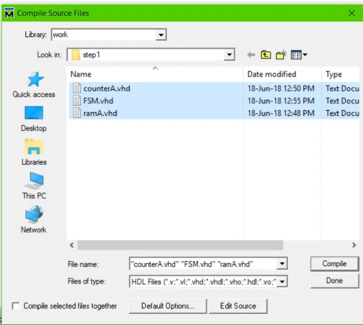
We first have to make sure that we compile all 3 files:
After that we run the simulation (ModelSim):

Interesting points:
- We reset the circuit by doing areset='1' (RESET state), which initializes the counter into "00".
- The FSM changes state (WRITEA) and we give various input values. The correct input is "1000". We see that the actual writing procedure is done in the "next cycle", which means the the first storage of RAM(A) happens in the 2nd cycle of WRITEA. The last storage happens in the RESET state, which is put by me for testing.
- At the point where I have a yellow line you can see that what gets written is '0' that had valid = '1', which is the value that we had before the rising edge event. Exactly at the event we change the value into '1' by also setting valid = '0'. In the end what gets written is not '1', but '0', which is the correct value.
- When valid = '1' the counter increments, but when valid = '0' the counter doesn't incerement and the RAM also doesn't get written (which would be pretty bad)
By all that we can see that the system works right until now, cause the reseting and writing works as it should. We have no "wrong" events happening. The worst would be having the wrong input get stored or having nothing at all being storedm, which are things that doesn't happen until now :D
Next time we will continue with step 2...
References:
- For the mathematical equations I used quicklatex!
- The code is all written by myself (it's a task for my University)
Previous posts of this series
- Part 1 -> problem, analysis, software model, architecture
And this is actually it for today's post! I will see you next time again where we will continue with step 2 of the implementation. There is a total of 4 parts, which means that I will try to get very in-depth into each "step"!
Bye!