
[Edit of Image1]
Introduction
Hey it's a me again @drifter1!
Today we continue with the Logic Design series on Verilog to get into Sequential Logic Examples. I was quite busy with the other series, and so I "skipped" this series for too long, but anyway. The examples in this article will be simple, commonly used sequential circuits (various flip flops, N-bit counter, single-port RAM), which will be implemented using procedural always blocks.
So, without further ado, let's get straight into it!
Flip Flops
Flip Flops and latches are commonly used circuits for storing state information, and the basic storage element in sequential logic. The change of state is controlled by one or more control inputs and the FF or latch has one or two outputs (which are mostly of inverted logic). Because Latches are mostly non-synthesizable I will again skip covering them. Now for Flips Flops, there is a wide variety of them, such as D, T, J-K and S-R. And those can even by broken down further, to be classified by an asynchronous or synchronous reset, control signal etc.
D Flip Flop (DFF)
Let's start with the most commonly used one, which is the D Flip Flop, short DFF. Considering a positive-edge triggered DFF, its input D is passed to the output Q, whenever the clock rises from 0 to 1. It's also quite common to include an asynchronous or synchronous reset, and sometimes there might even be an Q' output, which puts out the inverse of the input. Of course the input D, and output Q, can be of any length.
Let's go with the most basic case, with 1-bit inputs d, clk and reset, and 1-bit register output q. The module definition for that is:
module dff (output reg q, input d, clk, reset);
    /* main module */
endmodule
For a synchronous reset, the assign block is:
always @ (posedge clk) begin
    if (!reset)
        q <= 1'b0;
    else
        q <= d;
endalways @ (posedge clk or negedge reset) begin
if (!reset)
q <= 1'b0;
else
q <= d;
endT Flip Flop (TFF)
Next up, is the the T Flip Flop. For a positive-edge triggered TFF, the state toggles depending on the value of the control signal T. As such, the state is toggled (inverted) when the input is 1, on the rising edge event. In this case, the reset signal is required (and no longer optional), as the state simply inverts whenever T = 1. And, of course, the output state Q can be of any length.
Let's implement an 8-bit output T Flip Flop with synchronous reset. The module looks like this:
module tff (output [7 : 0] q, input t, clk, reset);

    reg [7 : 0] q_reg;
    assign q = q_reg;

    always @ (posedge clk) begin
        if (!reset)
            q_reg <= 0;
        else if (t)
            q_reg <= ~q_reg;
    end

endmoduleJ-K Flip Flop (JKFF)
We are now at one of the rare cases. A Just-Kidding (J and K don't stand for anything in particular) Flip Flop has the following truth table.

So, we could summarize that, during a rising edge clock event, the output stays the same when J = K = 0, toggles (inverts) when J = K = 1, and becomes the value of J, when J and K are not equal.
For 1-bit inputs J, K and output Q, and an asynchronous active-low reset, the module is written as follows:
module jkff (output q, input j, k, clk, reset);

    reg q_reg;
    assign q = q_reg;

    always @ (posedge clk or negedge reset) begin
        if (!reset)
            q_reg <= 0;
        else begin
            case ({j,k})
                2'b00 : q_reg <= q_reg;
                2'b01 : q_reg <= 0;
                2'b10 : q_reg <= 1;
                2'b11 : q_reg <= ~q_reg;
            endcase
        end
    end

endmoduleS-R Flip Flop (SRFF)
Another quite rare case, which is commonly used in Minecraft for some reason is the Set-Reset Flip Flop. I use such logic quite a lot in my redstone creations! Anyway, the truth table of the S-R Flip Flop is as follows.
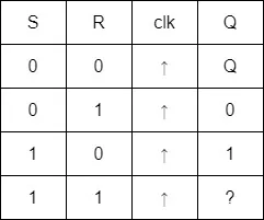
And so, basically, the output remains unchanged when R and S are both 0, is reset to 0 when R = 0, and set to 1 when S = 1. The behavior is unspecified for R = S = 1, but its common to keep the output unchanged. Thus, an S-R is basically an J-K Flip Flop without the inversion on R = S = 1.
The only change that needs to be made in the code is removing the ~ for the R = S = 1 case, and renaming the signals accordingly:
module srff (output q, input s, r, clk, reset);

    reg q_reg;
    assign q = q_reg;

    always @ (posedge clk or negedge reset) begin
        if (!reset)
            q_reg <= 0;
        else begin
            case ({s,r})
                2'b00 : q_reg <= q_reg;
                2'b01 : q_reg <= 0;
                2'b10 : q_reg <= 1;
                2'b11 : q_reg <= q_reg;
            endcase
        end
    end

endmodule
N-bit counter
Using the same logic as the various Flip Flops, its possible to implement N-bit counters, which count up, down, reset, are set to a specific input value, update only when an enable signal is active...you name it. Flip Flops, are very useful, and one should get into mastering them quickly!
So, how can the DFF code, be changed into a N-bit counter? Well, first of all, the data input is no longer necessary, except if there is a feature in the counter for setting it to a specific value. The initial value is set using the reset, be it asynchronous or synchronous, it doesn't matter. And, the counter, counts up, whenever the enable signal is active-high on a rising edge of the clock.
The code for an asynchronous reset counter with enable, is simply:
module counter (output [n - 1] q, input clk, reset, enable);

    reg [n - 1] q_reg;
    assign q = q_reg;

    always @ (posedge clk or negedge reset) begin
    if (!reset)
        q_reg <= 0;
    else if (enable)
        q_reg <= q_reg + 1;
    end

endmodule
Let's include a set signal and data input now, and also make the counter count up and down, by including a count_up signal. It might sound terrifying at first, but it's actually very easy to do!
The module definition changes into:
module counter (output [n - 1] q, input [n - 1] d, input clk, reset, enable, set, count_up);A new case, with any precedence that we wish for, needs to be added. For example, let's say the order is reset → set → enable. And, when enabled, there are now two sub-cases, which depend on the value of count_up. As such, the always block of the more advanced counter is:
always @ (posedge clk or negedge reset) begin
    if (!reset)
        q_reg <= 0;
    else if (set)
        q_reg <= d;
    else if (enable) begin
        if (count_up)
            q_reg <= q_reg + 1;
        else
            q_reg <= q_reg - 1;
    end
end
Single-Port RAM
Lastly, let's also get into how Random-Access Memory (RAM) can be modeled using the same principles.
One quite commonly used RAM implementation is the single-port RAM, with combined input and output (inout) data-line. One additional address-line is also defined, which specifies the location of the data (for reading) or where the data should be stored (for writing). As such, the circuit has a combined write/read enable control signal, as well as an output enable. And it's also common to have total chip select control signal, for deactivating the RAM as-a-whole. The array of memory to which the data is written, or the data is read from, is specified by a data width, address width and depth of elements (2address width).
I will not get into it too much, but this is how single-port ram can be implemented:
module single_port_ram(
        input clk,
        input [ADDR_WIDTH - 1 : 0],
        inout [DATA_WIDTH - 1 : 0],
        input cs,
        input we,
        input oe
    );

    reg [DATA_WIDTH - 1 : 0] mem [0 : DEPTH - 1];
    reg [DATA_WIDTH - 1 : 0] tmp_data;

    data = (cs & oe & !wr) ? tmp_data : 0;

    always @ (posedge clk) begin
        if (cs & we)
            mem[addr] <= data;
    end

    always @ (posedge clk) begin
        if(cs & !we)
            tmp_data <= mem[addr]
    end

endmoduleRESOURCES:
References
- http://www.asic-world.com/verilog/veritut.html
- https://www.chipverify.com/verilog/verilog-tutorial
- https://www.javatpoint.com/verilog
- http://www.cburch.com/logisim/docs/2.1.0/libs/mem/flipflops.html
Images
Previous articles of the series
- Verilog Introduction → Basic Syntax, Data Types, Operators, Modules
- Combinational Logic in Verilog → Assign Statement, Always Block, Control Blocks, Gate-Level Modeling and Primitives, User-Defined Primitives
- Combinational Logic Examples → One Circuit - Four Implementations, Encoder, Decoder, Multiplexer
- Sequential Logic → Procedural Blocks (Initial, Always), Blocking and Non-Blocking Assignments, Statement Groups
Final words | Next up
And this is actually it for today's post!
Next time we will get into Finite-State Machines (FSMs)...
See Ya!

Keep on drifting!